The price of failure: Dutch company's chip monopoly born from a bad bet by Intel
The price of failure: Dutch company's chip monopoly born from a bad bet by Intel
China or the US, who holds the real power in the global chip industry? Behind the investments in manufacturing giants such as Intel and TSMC is an assumption that whoever controls chip production has the power to direct the future of the global economy. But the real power may not be in the hands of the chip manufacturers themselves, but rather ASML, the company that owns the technology to manufacture the expensive machines that are used to manufacture the chips.
Who holds the real power in the global chip industry? An attempt to determine an answer to this question is at the heart of the chip war of the last two years, in which the U.S. imposed extensive sanctions on the export of chips and chip manufacturing technologies to China. China responded with its own sanctions, and the U.S., the European Union, Israel and other countries allocated tens of billions of dollars each In the form of grants to manufacturing giants such as Intel and TSMC with the goal of developing high-performance chip manufacturing facilities in their territory.
The assumption of these moves is that whoever controls the production of the chips has the power to direct the future of the field, and as a result the future of the global economy. But it is possible that the real power lies not in the production of the chips themselves, but in the hands of those who possess the technology to produce the expensive and complex machines that are used to produce the most advanced chips, which are at the heart of the generative artificial intelligence (GenAI) revolution, and which are needed for other advanced uses.
And this power is now almost exclusively in the hands of a Dutch company called ASML Holdings. And this, according to a Bloomberg analysis, as a result of fundamental mistakes made by the American government nearly 30 years ago, and a particularly bad bet by Intel about a decade and a half ago. The price of these mistakes is being paid by the U.S. and Intel to this day.
At the heart of the race for the development of advanced, faster and more powerful chips are efforts to make transistors as small as possible, with the aim of squeezing as many of them as possible into a smaller area. Today, the most advanced transistors are only a few nanometers in size. In the early decades of the chip industry, a process known as photolithography was used to create the transistors. This procedure used visible light to etch patterns in silicon substrates to create transistors. Later, the industry moved to ultraviolet light lithography, which allowed the creation of smaller transistors.
In the 1980s, scientists, first at the legendary Bell Labs in New Jersey and then at Department of Energy research institutes, began exploring the use of extreme ultraviolet lithography (EUV) to produce transistors at an atomic layer.
Throughout the 1990s, the Department of Energy invested tens of millions of dollars in this research, which was carried out at three national laboratories - Lawrence Livermore, Lawrence Berkeley, and Sandia, but the researchers soon realized that industry support was needed in order to develop the technology. In 1997, Intel, AMD and Motorola joined forces with the government in a public-private partnership and established an entity called EVU LLC with the aim of conducting basic research in the field, with the help of a private investment of a quarter of a billion dollars. As part of the agreement, the rights to use the research findings were fully owned by the U.S. government and distributed in accordance with the license granted by the Department of Defense. Later, a lithography company called Silicon Valley Group (SVG) was added to the project. At the same time, the Dutch ASML conducted a similar study in Europe, as did Nikon and Canon in Japan.
At that time, Nikon and Canon were considered the leading lithography companies in the world. However, against the background of fear of the dominance of Japanese companies in the global and American economy in particular, the Department of Defense decided not to grant them a license to use the technology, effectively making ASML and SVG the only players in the field, which was still in its infancy. In 2001, ASML acquired SVG in a deal worth $1.1 billion, becoming the only player attempting to develop EVU technology for commercial use.
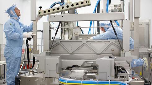
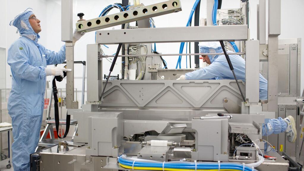
At the time, no one was bothered by it. The procedure itself is extremely complex and involves firing a powerful laser at a rate of 50,000 times per second in order to produce plasma that emits extreme ultraviolet light. This light does not exist naturally, and is also absorbed by the air, which necessitates its creation in a vacuum and the use of a mirror system for its absorption. The mirror system that ASML currently uses is manufactured by the German company Zeiss and its biggest flaw is only an atom in size. According to the company, if the mirror were the size of a country, the most prominent bump would be only a millimeter high. The production process itself is also complex, and the laser system requires frequent cleaning which involves prolonged downtime - a significant difficulty when it comes to a production facility whose construction cost tens of billions of dollars and which must operate around the clock in order to justify its activity.
Despite this, ASML estimated with the purchase of SVG that within five years the technology would reach commercial viability. As with similar breakthrough technologies, it was not until 2012 that the technology reached sufficient maturity for the industry to consider it practical. Even then, ASML still needed significant investments in order to enable the production and implementation of EVU machines on a significant scale. Its biggest customers, the chip manufacturers, were quick to mobilize: Samsung invested $974 million in the company, TSMC $1.4 billion and Intel $4.1 billion. These investments gave the three companies a quarter of ASML shares, with the lion's share going to Intel.
Two years later, ASML began manufacturing and marketing its EUV lithography machines on a large scale. And here, according to Bloomberg, Intel made a strategic mistake for which it is paying to this day. Despite the fact that it was the largest investor in the company, Intel chose not to receive any of ASML's first generation machines. This is because the CEO of Intel at the time, Brian Krzanich, feared that it would not be possible to economically justify their use, and preferred to continue with the existing technology until the various defects of the first generation could be addressed.
The one who benefited from this is TSMC, which was quick to adopt the technology and as a result was able, for the first time, to overtake Intel in its production capabilities. At the same time, Intel struggled to reliably implement its own alternative lithography technology, and by the time it was able to optimize the process on a large scale, TSMC and Samsung were already poised to produce even more advanced chips.
Intel pays the price of this mistake to this day. When it invested in ASML in 2012, Intel's market cap was 15 times that of Nvidia and 2 times that of TSMC. Today, Intel's value is $164 billion, while TSMC's is $650 billion while Nvidia has soared into the stratosphere with a $2.2 trillion valuation.
For the U.S., the resulting situation is particularly ironic. The new technology was based on scientific foundations developed in the U.S. and research funded by taxpayers and an American company. However, those who actually benefited from this research are companies in East Asia, one of which, TSMC, also sold the advanced chips it created to Chinese companies.
The technology that was American in its foundation and financing, was used to help its greatest economic and political rival. And if China continues to enjoy access to chips manufactured with EUV technology, or even obtains the ability to use the technology itself for the independent production of chips, it will be able to register significant leaps in the development of AI capabilities not only for private industry but also for military applications.
This concern is now at the root of the American embargo on the export of high-performance chips to China. But in light of ASML's monopoly on the technology used to manufacture these chips, the Biden administration also had to pressure the Dutch government to prohibit ASML from selling its production machinery to China. This pressure is taking its toll, for the time being, but the lack of direct U.S. control over this technology, which came to the world only thanks to its activity, is evidence of its weakness in the field and the strategic mistake made more than 20 years ago, in which the U.S.'s control over the technology was lost.
Intel, meanwhile, is determined not to miss the next breakthrough and is betting big on the next generation of EUV lithography, known as High Numerical Aperture EUV lithography, which uses light focused on an even smaller spot. Last December, Intel installed the first production systems based on the technology at the company's plant in Oregon. The technology may allow Intel to return to a leading position, but it will not change the balance of power behind the scenes: this technology is also developed, manufactured and controlled by ASML.


