Astera Labs expands global AI ambitions with new R&D center in Israel
Market-cap $28 billion firm taps local talent and Pliops assets to tackle next-generation AI connectivity challenges.
Astera Labs, a Nasdaq-listed developer of semiconductor connectivity solutions for AI infrastructure with a market capitalization exceeding $28 billion, has announced a major expansion of its global engineering operations with the launch of an advanced research and development center in Israel. The new facility, which will operate out of Tel Aviv and Haifa, aims to accelerate the development of next-generation scale-up fabrics for high-bandwidth connectivity and tackle memory bottlenecks that limit AI training and inference performance.
Although Astera Labs has not officially confirmed the origins of the new center, the expansion follows the acquisition of certain assets and intellectual property from Israeli startup Pliops. As part of the deal, approximately half of Pliops’ roughly 100 employees will join Astera Labs, while the remainder will be laid off. Around $70 million will be transferred to Pliops shareholders and employees, a sum significantly below the $215 million invested in the startup since its founding.
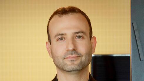
Guy Azrad, a veteran of the semiconductor industry, will lead the Israel operations as senior vice president of engineering and general manager. Azrad brings extensive experience in high-speed networking and compute technologies from prior leadership roles at Google and Marvell. “We’re building an engineering team with a strong focus on execution, covering hardware, silicon, and software solutions, to support the growing adoption of Astera Labs’ Intelligent Connectivity Platform,” Azrad said. “With offices in Tel Aviv and Haifa, the new design center will tap into the region's world-class engineering talent to focus on the full chip design flow, from architecture through production, including software and system design for cutting-edge AI fabrics and emerging inference applications.”
The Israel expansion also includes the recruitment of Ido Bukspan as vice president of ASIC engineering. Bukspan brings more than 20 years of semiconductor and networking experience from Mellanox Technologies, Nvidia, and Pliops. He has been instrumental in developing high-performance InfiniBand, Ethernet, and NVLink solutions that underpin modern AI infrastructure. “Israel has been defining networking innovation for decades,” Bukspan said. “I see the same drive, the same intensity to deliver highly performant connectivity solutions at Astera Labs. Together, we're taking AI connectivity to the next level.”
Astera Labs positions itself at the intersection of AI and high-speed connectivity, providing purpose-built solutions that integrate CXL, Ethernet, NVLink Fusion, PCIe, and UALink semiconductor technologies with its proprietary COSMOS software suite. This combination enables organizations to unify disparate components into flexible systems capable of handling both scale-up and scale-out AI workloads. By establishing a dedicated R&D hub in Israel, Astera Labs is seeking to address some of the most pressing technical challenges in AI infrastructure, including memory bottlenecks and high-bandwidth networking demands.


