










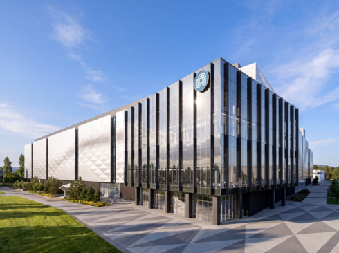
Applied Materials opens a $5 billion center to help build the next generation of AI chips
The EPIC Center is designed to bring chipmakers, equipment suppliers and university researchers together to develop manufacturing technologies in parallel, rather than through the traditional sequence of research and production handoffs.
The next breakthrough in AI chips may depend on getting the industry’s biggest rivals to work together. Applied Materials has opened a $5 billion research center in Silicon Valley where TSMC, Intel, Samsung and other semiconductor heavyweights will collaborate on technologies that are becoming harder and more expensive to develop, in a bid to move innovations from the lab to mass production faster.
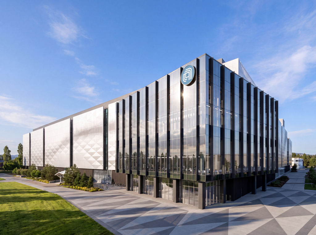
The U.S. semiconductor equipment maker has unveiled its new EPIC Center in Sunnyvale, California. The facility brings together some of the world’s largest chipmakers, equipment suppliers and university researchers to work alongside Applied Materials’ scientists and engineers on technologies intended for future generations of chips.
The founding partners include TSMC, Intel, Samsung Electronics, Micron Technology and SK hynix, companies that compete across parts of the semiconductor market. Broadcom, Advantest, SCREEN, Kioxia and Besi are among the innovation partners, alongside researchers from universities including Stanford, UC Berkeley, UCLA, Arizona State University and Rensselaer Polytechnic Institute.
The scale of the investment reflects the increasingly difficult engineering challenges posed by artificial intelligence. More powerful AI systems require advances not only in processors, but also in memory, the connections that move data between components and the packaging technologies that bring different elements together. Progress in one area increasingly depends on improvements in others.
Applied Materials, whose equipment is used in semiconductor manufacturing, sees an opportunity to make those developments more coordinated. Its EPIC Center, short for Equipment and Process Innovation and Commercialization, is designed to let teams develop materials, manufacturing equipment and production processes in parallel, rather than sequentially.
At EPIC, the company says, engineers from chipmakers and equipment suppliers will be able to work alongside the researchers developing the underlying technologies. Applied expects the model to shorten learning cycles and help customers move new processes into high-volume production sooner. Those benefits remain objectives of the project, rather than results that have yet been demonstrated publicly.
The facility itself spans approximately 600,000 square feet and includes nearly four acres of advanced cleanroom space. Applied says the construction required more than six million labor hours. The company expects capital spending to scale over time to approximately $5 billion as customer projects commence, rather than treating the entire sum as money already spent.